SEMICONDUCTOR DIODE
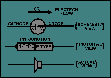
If we join a section of N-type semiconductor material with a similar section of P-type semiconductor material, we obtain a device known as a PN JUNCTION. (The area where the N and P regions meet is appropriately called the junction.) The usual characteristics of this device make it extremely useful in electronics as a diode rectifier. The diode rectifier or PN junction diode performs the same function as its counterpart in electron tubes but in a different way. The diode is nothing more than a two-element semiconductor device that makes use of the rectifying properties of a PN junction to convert alternating current into direct current by permitting current flow in only one direction. The schematic symbol of a PN junction diode is shown in figure 1-12. The vertical bar represents the cathode (N-type material) since it is the source of electrons and the arrow represents the anode. (P-type material) since it is the destination of the electrons. The label "CR1" is an alphanumerical code used to identify the diode. In this figure, we have only one diode so it is labeled CR1 (crystal rectifier number one). If there were four diodes shown in the diagram, the last diode would be labeled CR4. The heavy dark line shows electron flow. Notice it is against the arrow. For further clarification, a pictorial diagram of a PN junction and an actual semiconductor (one of many types) are also illustrated.
Figure 1-12. - The PN junction diode.
CONSTRUCTION
Figure 1-13. - Grown and fused PN junctions from which bars are cut.
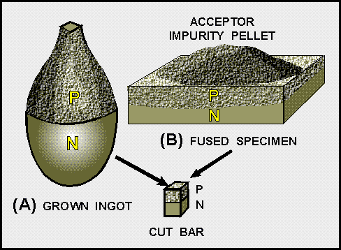
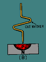
Figure 1-14A. - The point-contact type of diode construction.
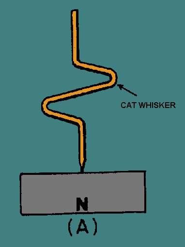
Figure 1-14B. - The point-contact type of diode construction.
Still another process is to heat a section of semiconductor material to near melting and then diffuse impurity atoms into a surface layer. Regardless of the process, the objective is to have a perfect bond everywhere along the union (interface) between P and N materials. Proper contact along the union is important because, as we will see later, the union (junction or interface) is the rectifying agent in the diode.
http://www.tpub.com/neets/book7/24f.htm
Jose Leonardo Moncada Torres
C.I 18878408
EES
No hay comentarios:
Publicar un comentario