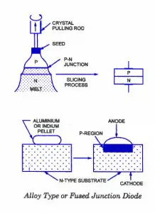
1. Grown Junction Diode: Diodes of this type are formed during the crystal pulling process. P and N-type impurities can be alternately added to the molten semiconductor material in the crucible, which results in a P-N junction, as shown when crystal is pulled. After slicing, the larger area device can then be cut into a large number (say in thousands) of smaller-area semiconductor diodes. Though such diodes, because of larger area, are capable of handling large currents but larger area also introduces more capacitive effects, which are undesirable. Such diodes are used for low frequencies.
2. Alloy Type or Fused Junction Diode: Such a diode is formed by first placing a P- type impurity (a tiny pellet of aluminium or some other P- type impurity) into the surface of an N-type crystal and heating the two until liquefaction occurs where the two materials meet. An alloy will result that on cooling will give a P-N junction at the boundary of the alloy substrate. Similarly, an N-type impurity may be placed into the surface of a P- type crystal and the two are heated until liquefaction occurs. Alloy type diodes have a high cur rent rating and large PIV (peak inverse voltage) rating. The junction capacitance is also large, due to the large junction area.
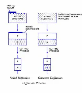
3. Diffused Junction Diode: Diffu sion is a process by which a heavy con centration of particles diffuse into a sur rounding region of lower concentration. The main difference between the diffu sion and alloy process is the fact that liquefaction is not reached in the diffu sion process. In the diffusion process heat is applied only to increase the activity of elements involved. For formation of such diodes, either solid or gaseous diffusion process can be employed. The process of solid diffusion starts with formation of layer of an acceptor impurity on an N- type substrate and heating the two until the impurity diffuses into the substrate to form the P-type layer, as illustrated in figure. A large P-N junction is divided into parts by cutting process. Metallic contacts are made for connecting anode and cathode leads.
In the process of gaseous diffusion instead of layer formation of an acceptor impurity, an N- type substrate is placed in a gaseous atmosphere of acceptor impurities and then heated. The impurity diffuses into the substrate to form P- type layer on the N- type substrate. Though, the diffusion process requires more time than the alloy process but it is relatively inexpensive, and can be very accurately controlled. The diffusion technique leads itself to the simultaneous fabrication of many hundreds of diodes on one small disc of semiconductor material and is most commonly used in the manufacture of semiconductor diodes. This technique is also used in the production of transistors and ICs (integrated circuits).
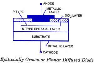
4. Epitaxial Growth or Planar Diffused Diode. The term “epitaxial” is derived from the Latin terms epi meaning ‘upon’ and taxis meaning “arrangement”.To construct an epitaxially grown diode, a very thin (single crystal) high impurity layer of semiconductor material (silicon or germanium) is grown on a heavily doped substrate (base) of the same material. This complete structure then forms the N- region on which P- region is diffused. Si02 layer is thermally grown on the top surface, photo-etched and then aluminium contact is made to the P- region. A metallic layer at the bottom of the substrate forms the cathode to which lead is attached.This process is usually employed in the fabrication of IC chips.
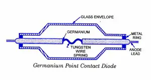
5. Point Contact Diode. It consists of an N-type germanium or silicon wafer about 12.5 mm square by 0.5 mm thick, one face of which is soldered to a metal base by radio-frequency heating and the other face has a phosphor bronze or tung sten spring pressed against it. A barrier layer is formed round the point contact by a pulsating current forming process. This causes a P-region to be formed round the wire and since pure germanium is N-type, a very small P-N junction in the shape of a hemisphere is formed round the point contact. The forming process cannot be controlled with precision. Because of small area of the junction, point contact diode can be used to rectify only very small currents (of the order of m A). On the other hand, the shunting capacitance of point contact diodes are very valuable in equipment operating at super high frequencies (as high as 25,000 MHz).
Source: http://www.circuitstoday.com/semiconductor-diode-fabrication-types


